- 您现在的位置:买卖IC网 > Sheet目录1996 > HMC703LP4E (Hittite Microwave Corporation)IC FRACT-N PLL W/SWEEPR 24QFN
p
ll
s
-
s
M
T
6 - 42
HMC703LP4E
v02.0813
8 GHz fractional syntHesizer
For price, delivery and to place orders: Hittite Microwave Corporation, 2 Elizabeth Drive, Chelmsford, MA 01824
978-250-3343 978-250-3373 fax Order On-line at www.hittite.com
Application Support: pll@hittite.com
serial Port open Mode Details
open Mode - serial Port Write operation
table 11. sPi open Mode - Write timing characteristics
Parameter
Conditions
Min.
Typ.
Max.
Units
t1
t2
t3
t4
t5
t6
sDI setup time
sDI hold time
sEN low duration
sEN high duration
sCK 32 Rising Edge to sEN Rising Edge
serial port Clock speed
sEN to sCK Recovery Time
3
10
DC
10
50
ns
MHz
ns
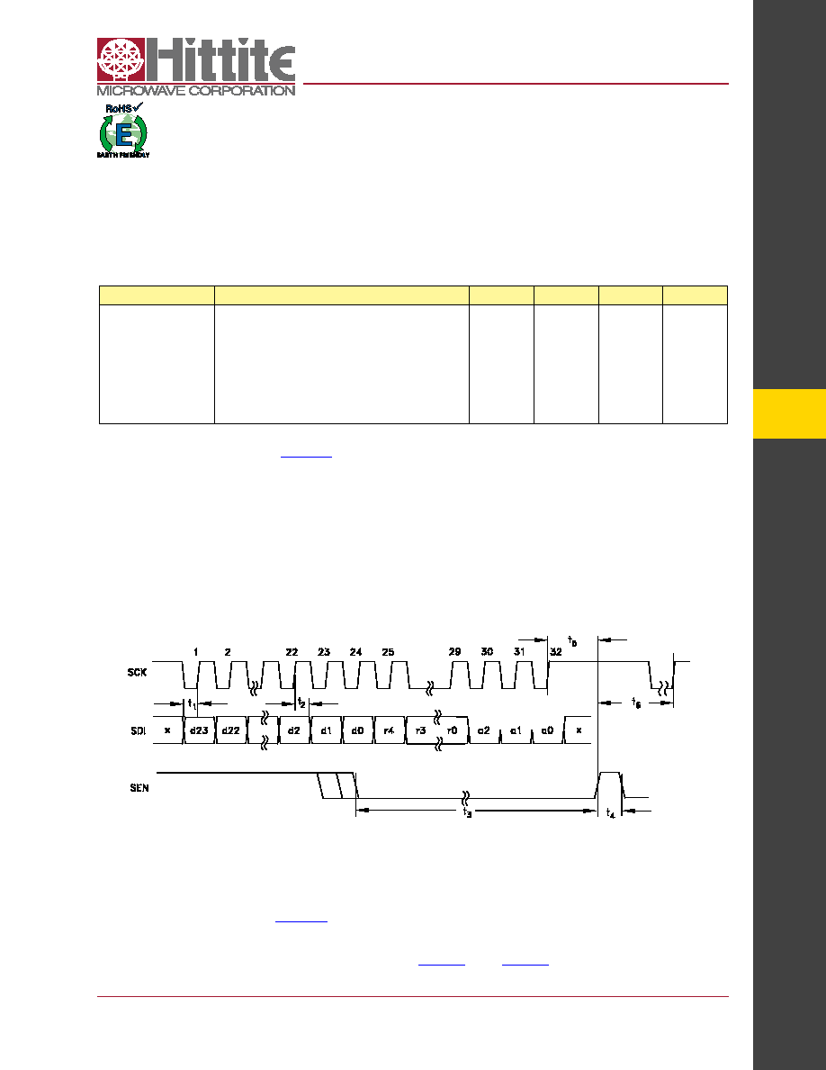
A typical WRITE cycle is shown in Figure 43.
a. The Master (host) places 24 bit data, d23:d0, MsB first, on sDI on the first 24 falling edges of sCK.
b. the slave (synthesizer) shifts in data on sDI on the first 24 rising edges of sCK
c. Master places 5 bit register address to be written to, r4:r0, MsB first, on the next 5 falling edges of
sCK (25-29)
d. slave shifts the register bits on the next 5 rising edges of sCK (25-29).
e. Master places 3 bit chip address, a2:a0, MsB first, on the next 3 falling edges of sCK (30-32). The
HMC703LP4E chip address is fixed at 000.
f.
slave shifts the chip address bits on the next 3 rising edges of sCK (30-32).
g. Master asserts sEN after the 32nd rising edge of sCK.
h. slave registers the sDI data on the rising edge of sEN.
Figure 43. Open Mode - Serial Port Timing Diagram - WRITE
open Mode - serial Port reaD operation
A typical READ cycle is shown in Figure 44.
In general, in Open Mode the LD_sDO line is always active during the WRITE cycle. During any Open Mode sPI cycle
LD_sDO will contain the data from the address pointed to by Reg 00h[4:0]. If Reg 00h[4:0] is not changed then the same
data will always be present on LD_sDO when an Open Mode cycle is in progress. If it is desired to READ from a spe-
发布紧急采购,3分钟左右您将得到回复。
相关PDF资料
HMC704LP4E
IC FRACT-N PLL 16BIT 24QFN
HMC830LP6GE
IC FRACT-N PLL W/VCO 40QFN
HMP8117CNZ
IC VIDEO DECODER NTSC/PAL 80PQFP
HMP8156ACNZ
IC VIDEO ENCODER NTSC/PAL 64MQFP
HSP45102SC-40Z
IC OSC NCO 40MHZ 28-SOIC
HSP45106JC-33Z
IC OSC NCO 33MHZ 84-PLCC
HSP45116AVC-52Z
IC OSC NCO 52MHZ 160-MQFP
ICL7109EPL+
IC ADC 12BIT 3-ST 40-DIP
相关代理商/技术参数
HMC703LP4ETR
制造商:Hittite Microwave Corp 功能描述:IC FRACT-N PLL W/SWEEPR 24QFN 制造商:Hittite Microwave Corp 功能描述:8 GHz Fractional-N PLL with Sweeper
HMC7043LP7FE
功能描述:IC FRACT-N PLL W/SWEEPR 48LFCSP 制造商:analog devices inc. 系列:- 包装:剪切带(CT) 零件状态:新产品 类型:* PLL:是 输入:时钟 输出:CML,LVDS,LVPECL 电路数:1 比率 - 输入:输出:1:14 差分 - 输入:输出:是/是 频率 - 最大值:3.2GHz 分频器/倍频器:是/无 电压 - 电源:3.135 V ~ 3.465 V 工作温度:-40°C ~ 85°C 安装类型:表面贴装 封装/外壳:48-VFQFN 裸露焊盘,CSP 供应商器件封装:48-LFCSP(7x7) 标准包装:1
HMC7043LP7FETR
功能描述:IC FRACT-N PLL W/SWEEPR 48LFCSP 制造商:analog devices inc. 系列:- 包装:剪切带(CT) 零件状态:在售 类型:时钟缓冲器 PLL:是 输入:时钟 输出:CMOS,LVDS,LVPECL 电路数:1 比率 - 输入:输出:1:14 差分 - 输入:输出:是/是 频率 - 最大值:3.2GHz 分频器/倍频器:是/无 电压 - 电源:3.135 V ~ 3.465 V 工作温度:-40°C ~ 85°C 安装类型:表面贴装 封装/外壳:48-VFQFN 裸露焊盘,CSP 供应商器件封装:48-LFCSP(7x7) 标准包装:1
HMC7044LP10BETR
功能描述:IC JITTER ATTENUATOR 68LFCSP 制造商:analog devices inc. 系列:- 包装:剪切带(CT) 零件状态:在售 类型:漂移衰减器 PLL:是 输入:CML,CMOS,LVDS,LVPECL 输出:CML,LVDS,LVPECL 电路数:1 比率 - 输入:输出:4:14 差分 - 输入:输出:是/是 频率 - 最大值:3.2GHz 分频器/倍频器:是/无 电压 - 电源:3.135 V ~ 3.465 V 工作温度:-40°C ~ 85°C 安装类型:表面贴装 封装/外壳:68-VFQFN 裸露焊盘,CSP 供应商器件封装:68-LFCSP-VQ(10x10) 标准包装:1
HMC704LP4E
功能描述:IC FRACT-N PLL 16BIT 24QFN RoHS:是 类别:集成电路 (IC) >> 时钟/计时 - 时钟发生器,PLL,频率合成器 系列:- 标准包装:2,000 系列:- 类型:PLL 频率合成器 PLL:是 输入:晶体 输出:时钟 电路数:1 比率 - 输入:输出:1:1 差分 - 输入:输出:无/无 频率 - 最大:1GHz 除法器/乘法器:是/无 电源电压:4.5 V ~ 5.5 V 工作温度:-20°C ~ 85°C 安装类型:表面贴装 封装/外壳:16-LSSOP(0.175",4.40mm 宽) 供应商设备封装:16-SSOP 包装:带卷 (TR) 其它名称:NJW1504V-TE1-NDNJW1504V-TE1TR
HMC704LP4ETR
制造商:Hittite Microwave Corp 功能描述:IC FRACT-N PLL 16BIT 24QFN
HMC705LP4
制造商:HITTITE 制造商全称:Hittite Microwave Corporation 功能描述:6.5 GHz PROGRAMMABLE DIVIDER (N = 1 - 17)
HMC705LP4E
制造商:Hittite Microwave Corp 功能描述:IC DIVIDER HBT PROGR 24-QFN